Eight boards to choose from, pin by pin: which GPIOs reach the header, which are input-only, which have an ADC, and which must be left alone.
Every project has one board, and it is always an ESP32 — the original chip, with two cores and Wi-Fi. The firmware and the compiler are the same on all eight models below. What changes is the header — which pins reach the edge of the board, with what label, and what else the board carries (a battery connector, a camera, an Uno shape). Choose the model on the board's card (double-click its title bar → Settings → Board model). Switching models keeps the wires that still have a pin to go to.
Which one to pick
Board
Pins
When
DOIT ESP32 DevKit V1 (30 pins)
30
The default and the most common board on the market — the one in most tutorials. The flash pins do not reach the header, and neither does GPIO 0.
ESP32-DevKitC V4 (38 pins)
38
Espressif's official board. Brings out 5 V, GPIO 0 and the flash GPIOs 6–11 (which must not be used — the lab crosses them out).
WROOM-32 module (no board)
38
The bare module, with no regulator and no USB. 3V3 is an input here: you supply regulated 3.3 V.
NodeMCU-32S (Ai-Thinker, 38 pins)
38
Ai-Thinker's 38-pin board: the DevKitC V4 layout with different labels — P in front of the GPIO, SVP/SVN, RX/TX. Very common in kits.
WeMos LOLIN32 Lite (26 pins)
26
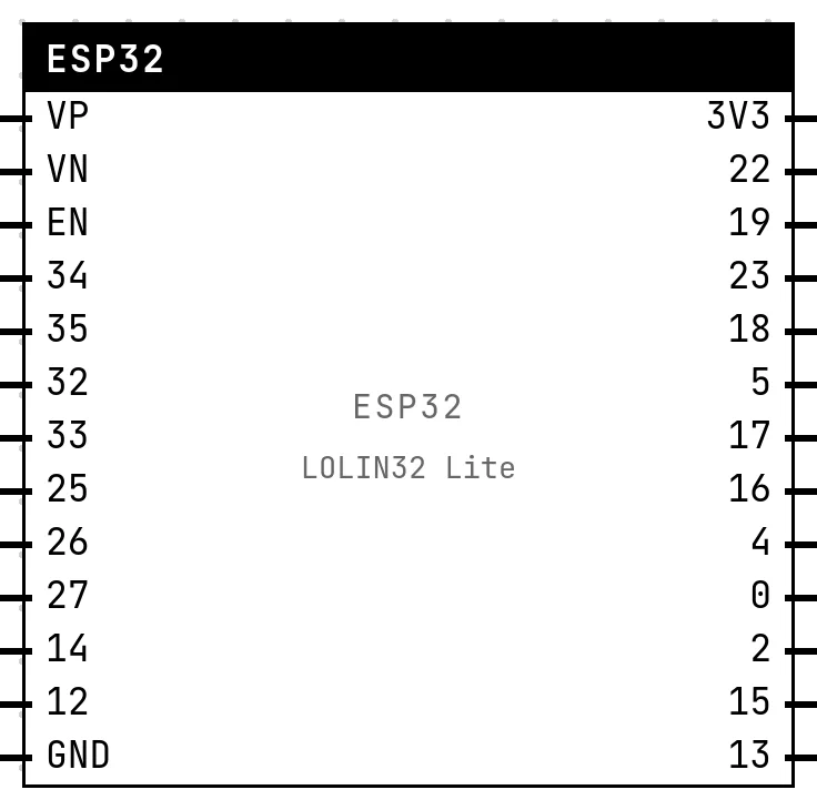
The small, cheap board with a Li-Po connector (“ESP32 Lite” in many shops). No 5 V pin, no RX0/TX0, no GPIO 21 on the header.
AI-Thinker ESP32-CAM (16 pins)
16
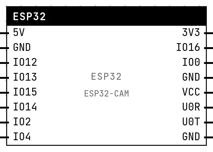
The camera board. The camera is simulated with your computer's camera (see the camera guide); the header has the 10 GPIOs left, the SD card on 2, 4, 12–15, no USB (programmed through U0R/U0T).
WeMos D1 R32 (Uno form factor)
30
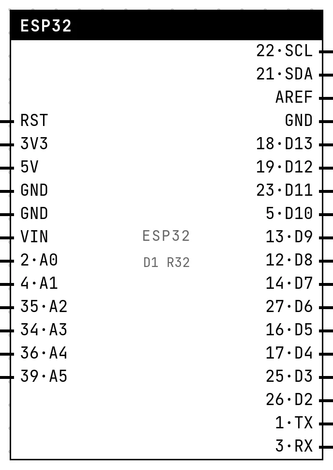
An ESP32 in the shape of an Arduino Uno, for Uno shields (at 3.3 V!). Pick it if your class has Uno shields on the shelf.
Adafruit HUZZAH32 Feather (28 pins)
28
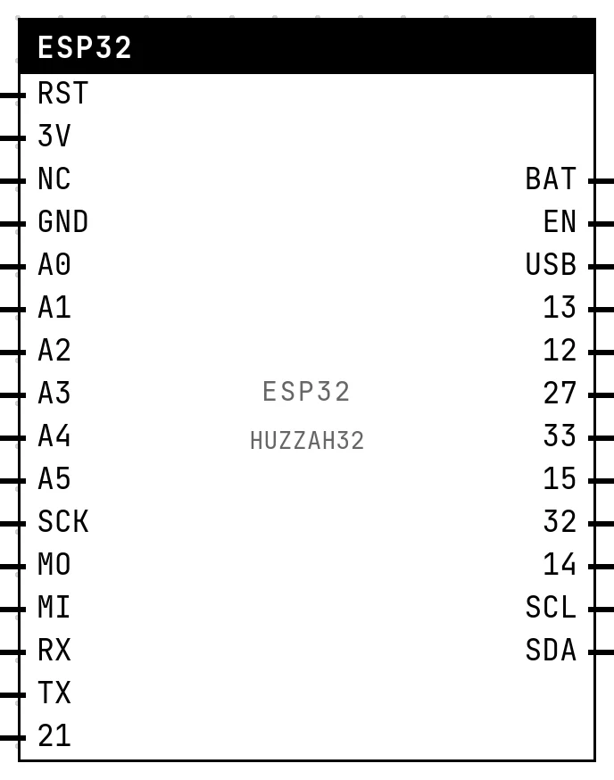
Adafruit's Feather: battery charging on board, the Feather pin layout, A0–A13 names. Common in the Adafruit ecosystem.
Rules that hold on every board
Everything is 3.3 V. A GPIO outputs 3.3 V and accepts at most 3.3 V. Wire 5 V into one and the lab shows a red warning — on a bench the pin is gone. The Uno-shaped board is no exception: its shields must be 3.3 V shields.
GPIOs 34, 35, 36 (VP) and 39 (VN) are input only, with no internal pull-up. They are the best pins for analog sensors, and useless for LEDs.
Any GPIO can be an ADC input? No: the ones marked ADC in the tables below can. The lab tells you if you wire a potentiometer to a pin without one.
GPIOs 6 to 11 belong to the flash chip. The 38-pin boards expose them; connecting anything there stops the chip from booting.
Strapping pins (0, 2, 12, 15) are read at boot to decide how the chip starts. They work as GPIOs, but avoid holding them at the wrong level while the chip resets.
I²C, SPI and Serial2 can use any GPIO — Wire.begin(sda, scl), SPI.begin(sck, miso, mosi), Serial2.begin(baud, config, rx, tx). The tables list the defaults that libraries assume when you give no pins.
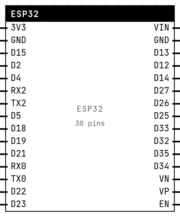
DOIT ESP32 DevKit V1 (30 pins)
The DOIT ESP32 DevKit V1 (30 pins) as the lab draws it, with the labels of the silkscreen.
Label
GPIO
Notes
3V3
3
RX0 — the serial monitor's receive line.
GND
—
Ground. All GND pins are the same node.
D15
15
ADC. Strapping pin; default CS of HSPI.
D2
2
ADC. Strapping pin; on many boards it also drives the on-board LED.
D4
4
ADC
RX2
16
RX2 — Serial2 receive by default (the GPS guide uses it).
TX2
17
TX2 — Serial2 transmit by default.
D5
5
Default chip select (CS) of the VSPI bus.
D18
18
Default SCK of VSPI (displays, SD card, LoRa).
D19
19
Default MISO of VSPI.
D21
21
Default SDA: Wire.begin() with no arguments uses it.
RX0
3
RX0 — the serial monitor's receive line.
TX0
1
TX0 — the serial monitor's transmit line. Using it as a GPIO breaks Serial.
D22
22
Default SCL: Wire.begin() with no arguments uses it.
D23
23
Default MOSI of VSPI.
VIN
—
5 V input to the regulator (what the USB supplies). Never wire it to a GPIO.
GND
—
Ground. All GND pins are the same node.
D13
13
ADC. Default MOSI of HSPI.
D12
12
ADC. Strapping pin: must be LOW at boot (the default MISO of HSPI).
D14
14
ADC. Default SCK of HSPI.
D27
27
ADC
D26
26
ADC. Also a DAC output on the real chip (not simulated).
D25
25
ADC. Also a DAC output on the real chip (not simulated).
D33
33
ADC
D32
32
ADC
D35
35
input only, no pull-up, ADC
D34
34
input only, no pull-up, ADC
VN
39
input only, no pull-up, ADC
VP
36
input only, no pull-up, ADC
EN
—
Chip enable: pulling it LOW holds the chip in reset.
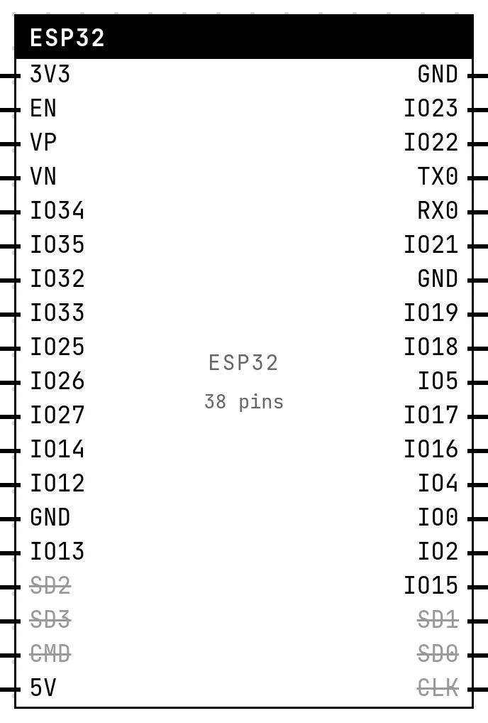
ESP32-DevKitC V4 (38 pins)
The ESP32-DevKitC V4 (38 pins) as the lab draws it, with the labels of the silkscreen.
Label
GPIO
Notes
3V3
3
RX0 — the serial monitor's receive line.
EN
—
Chip enable: pulling it LOW holds the chip in reset.
VP
36
input only, no pull-up, ADC
VN
39
input only, no pull-up, ADC
IO34
34
input only, no pull-up, ADC
IO35
35
input only, no pull-up, ADC
IO32
32
ADC
IO33
33
ADC
IO25
25
ADC. Also a DAC output on the real chip (not simulated).
IO26
26
ADC. Also a DAC output on the real chip (not simulated).
IO27
27
ADC
IO14
14
ADC. Default SCK of HSPI.
IO12
12
ADC. Strapping pin: must be LOW at boot (the default MISO of HSPI).
GND
—
Ground. All GND pins are the same node.
IO13
13
ADC. Default MOSI of HSPI.
SD2
9
internal flash — do not use
SD3
10
internal flash — do not use
CMD
11
internal flash — do not use
5V
5
Default chip select (CS) of the VSPI bus.
GND
—
Ground. All GND pins are the same node.
IO23
23
Default MOSI of VSPI.
IO22
22
Default SCL: Wire.begin() with no arguments uses it.
TX0
1
TX0 — the serial monitor's transmit line. Using it as a GPIO breaks Serial.
RX0
3
RX0 — the serial monitor's receive line.
IO21
21
Default SDA: Wire.begin() with no arguments uses it.
GND
—
Ground. All GND pins are the same node.
IO19
19
Default MISO of VSPI.
IO18
18
Default SCK of VSPI (displays, SD card, LoRa).
IO5
5
Default chip select (CS) of the VSPI bus.
IO17
17
TX2 — Serial2 transmit by default.
IO16
16
RX2 — Serial2 receive by default (the GPS guide uses it).
IO4
4
ADC
IO0
0
ADC. BOOT button, a strapping pin: leave it alone at boot; fine as an input afterwards.
IO2
2
ADC. Strapping pin; on many boards it also drives the on-board LED.
IO15
15
ADC. Strapping pin; default CS of HSPI.
SD1
8
internal flash — do not use
SD0
7
internal flash — do not use
CLK
6
internal flash — do not use
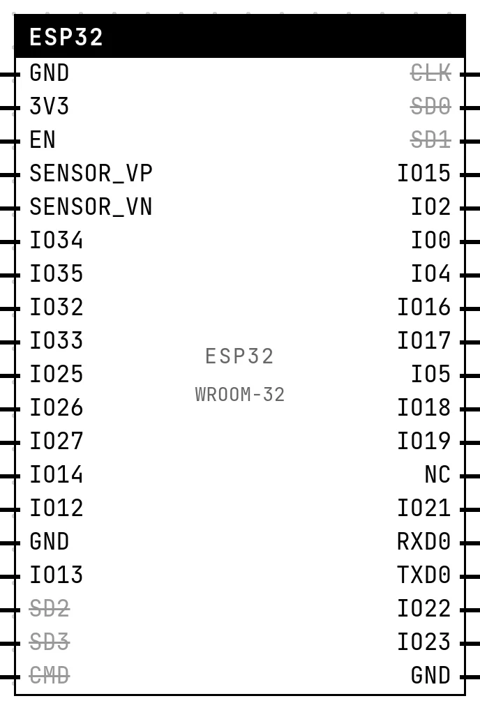
WROOM-32 module (no board)
The WROOM-32 module (no board) as the lab draws it, with the labels of the silkscreen.
Label
GPIO
Notes
GND
—
Ground. All GND pins are the same node.
3V3
3
RX0 — the serial monitor's receive line.
EN
—
Chip enable: pulling it LOW holds the chip in reset.
SENSOR_VP
36
input only, no pull-up, ADC
SENSOR_VN
39
input only, no pull-up, ADC
IO34
34
input only, no pull-up, ADC
IO35
35
input only, no pull-up, ADC
IO32
32
ADC
IO33
33
ADC
IO25
25
ADC. Also a DAC output on the real chip (not simulated).
IO26
26
ADC. Also a DAC output on the real chip (not simulated).
IO27
27
ADC
IO14
14
ADC. Default SCK of HSPI.
IO12
12
ADC. Strapping pin: must be LOW at boot (the default MISO of HSPI).
GND
—
Ground. All GND pins are the same node.
IO13
13
ADC. Default MOSI of HSPI.
SD2
9
internal flash — do not use
SD3
10
internal flash — do not use
CMD
11
internal flash — do not use
CLK
6
internal flash — do not use
SD0
7
internal flash — do not use
SD1
8
internal flash — do not use
IO15
15
ADC. Strapping pin; default CS of HSPI.
IO2
2
ADC. Strapping pin; on many boards it also drives the on-board LED.
IO0
0
ADC. BOOT button, a strapping pin: leave it alone at boot; fine as an input afterwards.
IO4
4
ADC
IO16
16
RX2 — Serial2 receive by default (the GPS guide uses it).
IO17
17
TX2 — Serial2 transmit by default.
IO5
5
Default chip select (CS) of the VSPI bus.
IO18
18
Default SCK of VSPI (displays, SD card, LoRa).
IO19
19
Default MISO of VSPI.
NC
—
Not connected.
IO21
21
Default SDA: Wire.begin() with no arguments uses it.
RXD0
3
RX0 — the serial monitor's receive line.
TXD0
1
TX0 — the serial monitor's transmit line. Using it as a GPIO breaks Serial.
IO22
22
Default SCL: Wire.begin() with no arguments uses it.
IO23
23
Default MOSI of VSPI.
GND
—
Ground. All GND pins are the same node.
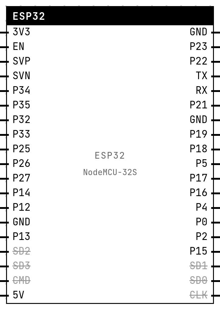
NodeMCU-32S (Ai-Thinker, 38 pins)
Physically the same 38-pin layout as the DevKitC V4 — the labels are what changes. SVP and SVN are GPIO 36 and 39 (the “sensor” inputs), RX/TX are the serial monitor's GPIO 3 and 1, and SD0–SD3, CMD and CLK are the flash pins: crossed out in the lab, off limits on the bench.
The NodeMCU-32S (Ai-Thinker, 38 pins) as the lab draws it, with the labels of the silkscreen.
Label
GPIO
Notes
3V3
3
RX0 — the serial monitor's receive line.
EN
—
Chip enable: pulling it LOW holds the chip in reset.
SVP
36
input only, no pull-up, ADC
SVN
39
input only, no pull-up, ADC
P34
34
input only, no pull-up, ADC
P35
35
input only, no pull-up, ADC
P32
32
ADC
P33
33
ADC
P25
25
ADC. Also a DAC output on the real chip (not simulated).
P26
26
ADC. Also a DAC output on the real chip (not simulated).
P27
27
ADC
P14
14
ADC. Default SCK of HSPI.
P12
12
ADC. Strapping pin: must be LOW at boot (the default MISO of HSPI).
GND
—
Ground. All GND pins are the same node.
P13
13
ADC. Default MOSI of HSPI.
SD2
9
internal flash — do not use
SD3
10
internal flash — do not use
CMD
11
internal flash — do not use
5V
5
Default chip select (CS) of the VSPI bus.
GND
—
Ground. All GND pins are the same node.
P23
23
Default MOSI of VSPI.
P22
22
Default SCL: Wire.begin() with no arguments uses it.
TX
1
TX0 — the serial monitor's transmit line. Using it as a GPIO breaks Serial.
RX
3
RX0 — the serial monitor's receive line.
P21
21
Default SDA: Wire.begin() with no arguments uses it.
GND
—
Ground. All GND pins are the same node.
P19
19
Default MISO of VSPI.
P18
18
Default SCK of VSPI (displays, SD card, LoRa).
P5
5
Default chip select (CS) of the VSPI bus.
P17
17
TX2 — Serial2 transmit by default.
P16
16
RX2 — Serial2 receive by default (the GPS guide uses it).
P4
4
ADC
P0
0
ADC. BOOT button, a strapping pin: leave it alone at boot; fine as an input afterwards.
P2
2
ADC. Strapping pin; on many boards it also drives the on-board LED.
P15
15
ADC. Strapping pin; default CS of HSPI.
SD1
8
internal flash — do not use
SD0
7
internal flash — do not use
CLK
6
internal flash — do not use
WeMos LOLIN32 Lite (26 pins)
Two rows of thirteen. One row starts with VP and ends with the only GND; the other starts with the only 3V3 and ends with 13. There is no 5 V pin: the board is powered by the USB or by the battery on its connector. GPIO 21, the usual SDA, is not on the header — call Wire.begin(19, 23) or any other pair. The blue LED on the board is GPIO 22, and it lights on LOW.
The WeMos LOLIN32 Lite (26 pins) as the lab draws it, with the labels of the silkscreen.
Label
GPIO
Notes
VP
36
input only, no pull-up, ADC
VN
39
input only, no pull-up, ADC
EN
—
Chip enable: pulling it LOW holds the chip in reset.
34
34
input only, no pull-up, ADC
35
35
input only, no pull-up, ADC
32
32
ADC
33
33
ADC
25
25
ADC. Also a DAC output on the real chip (not simulated).
26
26
ADC. Also a DAC output on the real chip (not simulated).
27
27
ADC
14
14
ADC. Default SCK of HSPI.
12
12
ADC. Strapping pin: must be LOW at boot (the default MISO of HSPI).
GND
—
Ground. All GND pins are the same node.
3V3
3
RX0 — the serial monitor's receive line.
22
22
Default SCL: Wire.begin() with no arguments uses it.
19
19
Default MISO of VSPI.
23
23
Default MOSI of VSPI.
18
18
Default SCK of VSPI (displays, SD card, LoRa).
5
5
Default chip select (CS) of the VSPI bus.
17
17
TX2 — Serial2 transmit by default.
16
16
RX2 — Serial2 receive by default (the GPS guide uses it).
4
4
ADC
0
0
ADC. BOOT button, a strapping pin: leave it alone at boot; fine as an input afterwards.
2
2
ADC. Strapping pin; on many boards it also drives the on-board LED.
15
15
ADC. Strapping pin; default CS of HSPI.
13
13
ADC. Default MOSI of HSPI.
AI-Thinker ESP32-CAM (16 pins)
Drawn with the camera connector at the top and the SD slot facing you. The camera is simulated: with this board, esp_camera_fb_get() gets frames from your computer's camera, degraded to the configured size and JPEG quality — see ESP32-CAM camera. Only ten GPIOs reach the header: the camera takes fifteen, all of them off-board. Of the ten, 2, 4, 12, 13, 14 and 15 are also the SD card's lines — wire a sensor there and the card stops working — and 4 drives the white flash LED. U0R and U0T are GPIO 3 and 1, the serial port you program the board through; VCC is the 3.3 V output of the on-board regulator.
The AI-Thinker ESP32-CAM (16 pins) as the lab draws it, with the labels of the silkscreen.
Label
GPIO
Notes
5V
5
Default chip select (CS) of the VSPI bus.
GND
—
Ground. All GND pins are the same node.
IO12
12
ADC. Strapping pin: must be LOW at boot (the default MISO of HSPI).
IO13
13
ADC. Default MOSI of HSPI.
IO15
15
ADC. Strapping pin; default CS of HSPI.
IO14
14
ADC. Default SCK of HSPI.
IO2
2
ADC. Strapping pin; on many boards it also drives the on-board LED.
IO4
4
ADC
3V3
3
RX0 — the serial monitor's receive line.
IO16
16
RX2 — Serial2 receive by default (the GPS guide uses it).
IO0
0
ADC. BOOT button, a strapping pin: leave it alone at boot; fine as an input afterwards.
GND
—
Ground. All GND pins are the same node.
VCC
—
U0R
3
RX0 — the serial monitor's receive line.
U0T
1
TX0 — the serial monitor's transmit line. Using it as a GPIO breaks Serial.
GND
—
Ground. All GND pins are the same node.
WeMos D1 R32 (Uno form factor)
The two Uno headers become the two columns: on the left the power and analog header (RST, 3V3, 5V, GND, VIN, then A0–A5), on the right the digital one (SCL, SDA, AREF, GND, then D13 down to D0). Each label carries the GPIO and the Uno name (“26·D2”), because the board prints both. Two silkscreen errors on the real board: A2 is printed “IO36” but is GPIO 35, and A4 is printed “IO38” — a pin that does not exist — but is GPIO 36. The lab shows the real GPIO. The on-board LED is GPIO 2, which is also A0.
The WeMos D1 R32 (Uno form factor) as the lab draws it, with the labels of the silkscreen.
Label
GPIO
Notes
RST
—
Chip enable: pulling it LOW holds the chip in reset.
3V3
3
RX0 — the serial monitor's receive line.
5V
5
Default chip select (CS) of the VSPI bus.
GND
—
Ground. All GND pins are the same node.
GND
—
Ground. All GND pins are the same node.
VIN
—
5 V input to the regulator (what the USB supplies). Never wire it to a GPIO.
2·A0
2
ADC. Strapping pin; on many boards it also drives the on-board LED.
4·A1
4
ADC
35·A2
35
input only, no pull-up, ADC
34·A3
34
input only, no pull-up, ADC
36·A4
36
input only, no pull-up, ADC
39·A5
39
input only, no pull-up, ADC
22·SCL
22
Default SCL: Wire.begin() with no arguments uses it.
21·SDA
21
Default SDA: Wire.begin() with no arguments uses it.
AREF
—
Not connected.
GND
—
Ground. All GND pins are the same node.
18·D13
18
Default SCK of VSPI (displays, SD card, LoRa).
19·D12
19
Default MISO of VSPI.
23·D11
23
Default MOSI of VSPI.
5·D10
5
Default chip select (CS) of the VSPI bus.
13·D9
13
ADC. Default MOSI of HSPI.
12·D8
12
ADC. Strapping pin: must be LOW at boot (the default MISO of HSPI).
14·D7
14
ADC. Default SCK of HSPI.
27·D6
27
ADC
16·D5
16
RX2 — Serial2 receive by default (the GPS guide uses it).
17·D4
17
TX2 — Serial2 transmit by default.
25·D3
25
ADC. Also a DAC output on the real chip (not simulated).
26·D2
26
ADC. Also a DAC output on the real chip (not simulated).
1·TX
1
TX0 — the serial monitor's transmit line. Using it as a GPIO breaks Serial.
3·RX
3
RX0 — the serial monitor's receive line.
Adafruit HUZZAH32 Feather (28 pins)
The long side is the Feather standard: RST (the chip's reset), 3V from the regulator, A0–A5, then SPI (SCK 5, MO 18, MI 19), serial (RX 16, TX 17) and GPIO 21. The short side has BAT (the Li-Po, not modeled), EN (the regulator's enable, not the chip's) and USB (5 V from the connector — wiring it to a GPIO gets the red warning), then 13, 12, 27, 33, 15, 32, 14 and I²C on SCL 22 and SDA 23. The red LED is GPIO 13; A13 (GPIO 35) reads half the battery voltage.
The Adafruit HUZZAH32 Feather (28 pins) as the lab draws it, with the labels of the silkscreen.
Label
GPIO
Notes
RST
—
3V
3
RX0 — the serial monitor's receive line.
NC
—
Not connected.
GND
—
Ground. All GND pins are the same node.
A0
26
ADC. Also a DAC output on the real chip (not simulated).
A1
25
ADC. Also a DAC output on the real chip (not simulated).
A2
34
input only, no pull-up, ADC
A3
39
input only, no pull-up, ADC
A4
36
input only, no pull-up, ADC
A5
4
ADC
SCK
5
Default chip select (CS) of the VSPI bus.
MO
18
Default SCK of VSPI (displays, SD card, LoRa).
MI
19
Default MISO of VSPI.
RX
16
RX2 — Serial2 receive by default (the GPS guide uses it).
TX
17
TX2 — Serial2 transmit by default.
21
21
Default SDA: Wire.begin() with no arguments uses it.
BAT
—
EN
—
Chip enable: pulling it LOW holds the chip in reset.
USB
—
13
13
ADC. Default MOSI of HSPI.
12
12
ADC. Strapping pin: must be LOW at boot (the default MISO of HSPI).
27
27
ADC
33
33
ADC
15
15
ADC. Strapping pin; default CS of HSPI.
32
32
ADC
14
14
ADC. Default SCK of HSPI.
SCL
22
Default SCL: Wire.begin() with no arguments uses it.
SDA
23
Default MOSI of VSPI.
See also
Placing parts and wiring — The catalog, the Wire tool, junctions and free tracks, nets and their colors, the ground and power symbols, and the tools that move, rotate and delete.
Power, ground and the voltmeter — The GND and 3V3 symbols, the adjustable power supply, the voltmeter, and the electrical warnings the lab raises when a wire would damage the board.